Two key innovations
The combination of two key innovations create an easy to manufacture die that contains all of the optical functionality for a spectrometer. These dies are fabricated at the wafer scale using scalable processes, and have a simple stacked alignment to the detector.
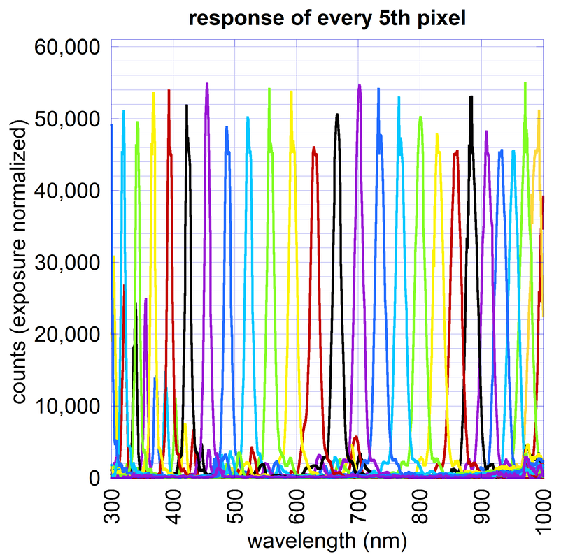
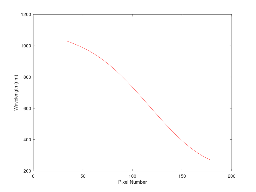
The Chromation Spec dev kit is the first product that uses the combination of photonic crystals and a folded optical path. The plots below show response data measured from one of the dev kits. More information on the Chromation Spec dev kit is available here.
The video below demonstrates the simplicity of this architecture by showing the response of one of our optical dies placed on an ordinary cell phone camera. In the video, an optical die is place on the phone's front camera. The real time responses to ambient light and different LED sources are seen on the phone's display.
Advantages
Usability
|
Manufacturability
|
Roadmap
Our current products are the first demonstration of our technology. Our roadmap covers a number of initiatives to further reduce size and expand capabilities including the move to surface mount chip packaging and extension further into the NIR.